Reverse Engineering Firmware (in Mice)
Streaming Video from the Mouse
Previously, I
- reverse engineered the encryption used in the sensor (ADNS-9800) by staring at it really hard
- reverse engineered parts of the sensor firmware
Before that, I also reverse engineered parts of the USB controller firmware of the mouse. When looking into the ADNS-9800 datasheet, one is presented with the possibility of reading 30x30 greyscale images from the device, so I decided to just do that.
Hello World!
As far as I know, the pre-existing USB controller firmware does not have any built-in function to read the frames, which is not really surprising. So I will have to modify the firmware. When patching binaries, I find doing so in assembly is often advantageous to C (or PL/M-51, which is never advantageous) because it allows to modify existing functions or jump to the middle of a function. I’m also quite used to 8051 assembly, so writing it poses no problem.
To not risk break existing USB functionality
- I copied the existing routines for the recovery USB mode to a separate location
- I made minimal modifications to the rest of the firmware (basically replacing one jump address) to invoke it
If the new mode is invoked, all interrupts are disabled and it is in a busy-wait loop waiting for USB packets.
First, of course, I wrote a simple hello world function that returns the string Hello, World!\n
on a GET_REPORT:
	MOV DPTR, #USB_OUT	; init dptr with USB buf address
	MOV A, #03		; report id, start of get_report
	MOV R0, #08		; number of bytes in buffer left
	MOV R1, #(HELLO-PC_VA1)	; offset to "hello world" string
	MOV R2, #00		; FFh at second batch of 8 bytes
COPY_LOOP:
	MOVX @DPTR, A
	INC DPTR
	MOV A, R1
	MOVC A, @A+PC
PC_VA1: INC R1
	DJNZ R0, COPY_LOOP
	XCH A, R2
	JNZ SEND
	LCALL ADV_USB
	MOV R0, #08
	CPL A
	XCH A, R2
	MOV DPL, #08
	SJMP COPY_LOOP
SEND:
	LCALL ADV_USB
	LJMP ADV_USB
HELLO:	DB 'Hello, World!', 10, 0
This works without problem, and one gets to test both the firmware code and host code for invoking the special mode.
Knowing that the hello world
works, I could now go on to read frames from the sensor.
Reading Frames and Optimizing FPS
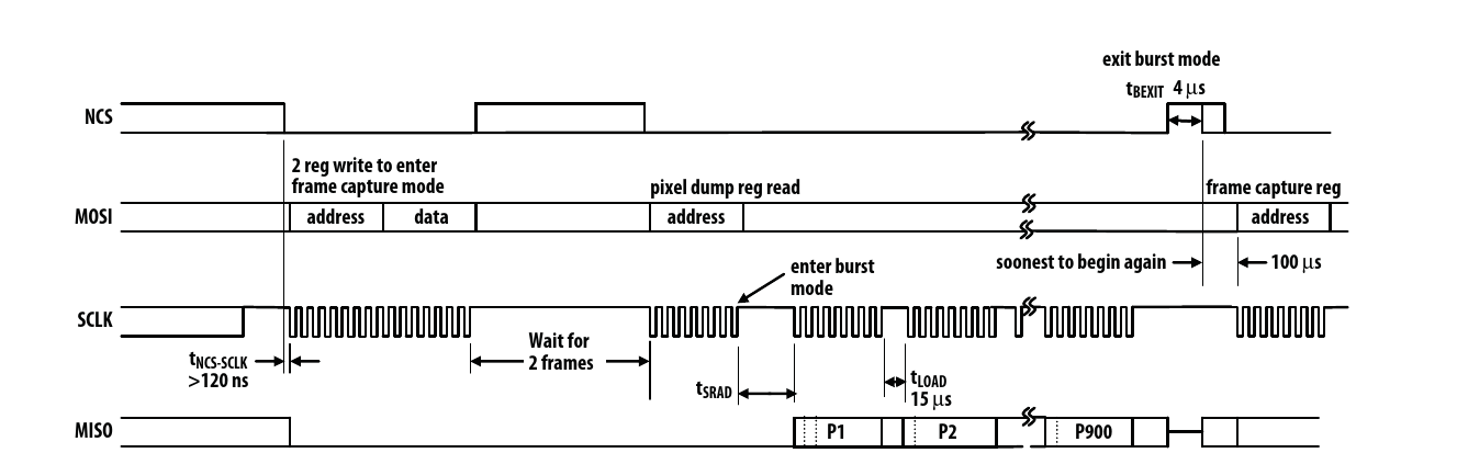
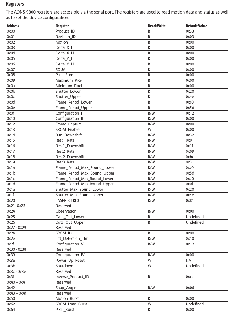
The ADNS-9800 communicates over SPI, but the USB controller doesn’t have any native SPI ports, so it has to bit-bang the frames. Communication involves registers, which can be read or written to by sending the address over SPI and then reading/writing the byte. Getting the frame involves writing some values to a register and then reading 900 bytes from another register, all over SPI.
A peculiarity about the USB controller is that, in order to set some I/O lines high or low, other bits have to be set or unset. I’m not sure what exactly it does, but it does not work when skipping it.
On the first try, I implemented it on the USB controller by storing the frame inside an XRAM buffer and reading that into the USB buffer.
The host side was made using a PyQT application that sends the GET_REPORT requests and displays it inside a GUI.
Needless to say, the step of copying it to a buffer made it quite slow and I got somewhere along 7fps.
After moving the USB communication logic to a separate thread, eliminating the buffer and a bunch of micro-optimizations, I already increased the fps to 17fps. Of course, no one will be satisfied with just 17fps. But what next?
Well, one easy thing to do is to just ignore the timings given by the data sheet and removing as many sleeps in the firmware as possible. Another thing drastically improving performance is loop unrolling: In the innermost loop for the bit-banging, the code was
	MOV A, #1
BURST_READ:
	PORT_L SCLK
	PORT_H SCLK
	MOV C, MISO
	RLC A
	JNC BURST_READ		; until whole byte is read
Of course, since a byte will always be 8 bits on an 8051, it is faster to leave the JNC out and instead repeat the snippet 8 times.
Since this is an 8051, there is also no instruction cache to consider (I’ve never seen an 8051 with an instruction cache).
With this done, the fps is already at 34 fps, double of the previous value.
One thing that prevented me from doing some micro-optimizations, however, is that I didn’t know the exact instruction timings:
most 8051 instructions (barring maybe conditional jumps or div ab) on most cores have a constant number of cycles to be executed.
In order to find that out, I made this piece of 8051 code.
I stuffed almost every instruction (up to registers) inside 256 bytes because I wanted to jump using a single jmp @a+dptr without doing 16-bit arithmetic, which would make the overhead higher and measurement harder.
This involved stuffing instructions into arguments of other instructions, so that they’re effectively shingled.
The hardest part of this was getting other instructions into the relative jump instructions:
they still had to branch to return instructions, but moving other instructions would change the distribution of return instructions.
In the end, it produced accurate measurements after looping a million times for each instruction type.
It turns out that the clock is probably 12MHz (if nop takes one cycle).
More surprising is the fact that setb [bit] takes 3 cycles while mov [direct], [ri] takes 2 cycles.
It means that bit-banging the clock using setb actually takes 1.5 times as long as mov.
Setting the clock pin high and low with mov doesn’t actually require reading out the previous state and or’ing/and’ing it:
the only changed pin is SCLK and MISO is read from the input latch so in the output, this is actually 0.
I thus saved the predicted states inside some registers and moved them to the ports when desired.
Other instructions I’ve misestimated are the ret (8 cycles) and lcall/acall (7 cycles) instructions.
In general, the timings on this core were all over the place, but at least the da a instruction was 1 cycle, for all your fast decimal adjustment needs.
Anyway, the time taken for one transmitted bit went down from 17 cycles to 11 cycles, quite an improvement.
Another improvement was inlining the function responsible for advancing the USB buffer to the next 8 bytes. There was also some improvement to be made by removing some instructions. Before the magical incantation to advance the buffer was:
	ORL 086h, #040h
	ORL 086h, #040h
	ANL 09Dh, #0F0h
	ORL 09Dh, #008h
	ANL 086h, #03Fh
	ORL 086h, #040h
	ORL 098h, #004h
	ANL 086h, #03Fh
	ANL 086h, #03Fh
	ORL 086h, #040h
BUSY_WAIT:
	MOV A, #098h
	JB ACC.2, BUSY_WAIT

	ANL 086h, #03Fh
It can be shortened to
	ORL 086h, #040h
	ORL 086h, #040h
	ANL 09Dh, #0F0h
	ORL 09Dh, #008h
	ORL 098h, #004h
BUSY_WAIT:
	JB 098h.2, BUSY_WAIT
	ANL 086h, #040h
	ANL 086h, #040h
One might think that the double ORL 086h, #040h or double ANL 086h, #040h can be combined to one, but that is not the case.
I guess it might be responsible for changing SFR banks, but it’s not really clear to me.
Another thing was that BUSY_WAIT loop:
it actually ate quite a bit of time.
Instead of waiting for the transfer to end right after initiating it, I buffered the 8 read bytes in IRAM and moved the busy loop before the transfer of the next loop.
Frame bytes from the sensor are instead buffered into IRAM.
The IRAM bytes are then moved into the USB buffer after the busy wait loop, and the next transfer is initiated.
The fps was now at a whopping 54fps and with the delays of the ADNS-9800 and the bit-banging, there’s not much left to do, right? No, of course not, what do you even expect when the scrollbar has not even reached half? I haven’t touched the ADNS-9800 firmware itself yet.
Optimizing by Modifying Sensor Firmware
The ADNS-9800 internally has 5 different interrupts. The interrupt vector itself is (probably) part of the mask ROM, which can’t be changed. But the interrupts themselves are just calling an address loaded from XRAM. This allows the patch ROM to change interrupt logic.
By inserting a counter for each interrupt and leaving the rest of the firmware in normal operation, the individual interrupt rates are counted. The result is
- once per register r/w for interrupt 5
- never for interrupt 4 (which is a stub)
- once per frame for interrupt 1-3
But when making fast code, time is insufficient for an interrupt to hit every frame (there are up to 12000 a second) and the response time for the I/O interrupt is too long. Therefore, polling instead of using interrupts seemed like the sensible thing to do. There is one hindrance: The existing interrupts can’t be used, so a deeper understanding of the underlying hardware is needed.
Fortunately, everything needed was just a way to get the frame and to communicate with the USB controller. The SPI interface is simple, 2 bits in an SFR signifying r/w, one SFR for the register address and one SFR for reading/writing. Figuring out how to get frames, however, proved difficult.
To start with, the function that outputs the frame to the SPI is just copying them from 0xC006 and after.
Clearly, the frames had to be copied there before, so the next place to look would be the register for triggering a new frame.
Still, all it does is set an SFR and some status bits.
The status bits get picked up by interrupts, which again set more SFRs and further status bits.
Similarly, further actions get triggered from those.
Figuring out what the SFRs do individually just by looking at the firmware was too hard. But it became clear that it was not the 8051 putting the frame bytes in memory. One of the SFRs set was probably responsible for activating that.
Trying them out seemed like a good idea.
Luckily, the ADNS-9800 has many reserved
registers that are in fact for debugging.
The debug interface has following functionality:
0x30: Write0x44to enable debug0x31: lower debug address byte0x32: upper debug address byte0x33: access XRAM (or IRAM when addr <0x100)0x34:0x33but postincrement addr0x35: access ROM with base address0xC006, postincrement0x36: access ROM0x44: set SFR read address0x45: set SFR write address0x46: execute SFR read/write- Some more which was not interesting or I didn’t figure out
Notice how the firmware and frames are loaded at address 0xC006 and not at a more reasonable 0xC000?
That’s because the first 6 bytes get used for the SFR debug functionality.
The 8051 has no way to indirectly address SFRs, so the firmware writes a small function containing the mov to/from the SFR, which is 6 bytes in size.
Anyway, after some testing using the debug functionality, I found out that the MSB of the SFR 0xEE activates the frame writing.
If it is not deactivated, it just keeps cyclically writing frames to the 3kB following the frame location.
This does mean that the frame has to properly timed to deactivate the bit in time.
Fortunately, one of the interrupts that fires every frame behaves like one of the traditional 8051 external interrupts, meaning IE0 get sets when it fires, making polling possible.
Another problem is that the location where the firmware is uploaded is occupied by frames. Something I’ve not mentioned yet is the existence of 1 kilobyte of XRAM memory mapped at 0x8000. It turns out to also be mapped to the code ROM.
Firmware could therefore alternatively be uploaded to XRAM with the debug port.
Executing it can be done through debug register 0x46, which just calls 0xC000.
By not using 0x44/0x45 but writing own code there through 0x36, it could jump to 0x8000.
Since writes to SPI are handled in interrupt context, I needed a way out. Fortunately, the original firmware already provide the needed functionality: It can write a configurable address to the bottom of the stack (used for resets). This way, at some point in the future, execution will return to that address, and it will not be in interrupt context, since an interrupt always writes a return address to the stack.
Having gotten that out of the way, the actual firmware could be written. It was quite simple, poll for new read from SPI, immediately copy new byte to output when that happens and then update counters. During the first 7 rows of a frame (each 30 pixels), buffer the content of the last 7 rows into IRAM. For the last 7 rows of a frame, enable MSB of 0xEE to get new frame and intermittently poll to see if frame complete and disable MSB of 0xEE. Since they are buffered, the pixels of the current frame can still be read even though the ones in the original locations are overwritten.
This way, the delay for a new frame is eliminated, as it is already done in the previous frame. Polling for reads is done in a tight busy wait, so no delay for the USB controller there either.
Since the data from the new ADNS-9800 firmware is one continuous data stream, I changed the USB controller to use 2kB packets to reduce overhead.
I also changed the host software from python to rust and made multiple threads spamming GET_REPORTS at the mouse.
As a result of all this, the fps is now at a blazingly fast 100fps. But what if it was even faster?
Not much can be done in the USB controller, all sleep calls are eliminated and the bit-banging loop offers only small improvements (unless I could eliminate the fact that two bits need to be changed to drive the clock). But after measuring the instructions cycles on the ADNS-9800, it has 50MHz and is therefore quite a bit faster than the USB controller. You know what this means? It’s image compression time!
Compression
So what image compression could be used for an 8051 running at 50 MHz with barely any free space? I chose a simple lossless compression that works like this:
- Decorrelation: take the difference between the current pixel and the (floored) average of the top and left pixel This way, the distribution of values is around 0 and has a small deviation, which is useful for the next step.
- Huffman compression: Map each value to a sequence of bits such that more common values have shorter bit sequences and it can be uniquely decoded
Note that in the decorrelation step, if it is the first column/row, one can simple do the difference without an average in just one direction. And the very first pixel can just be transmitted without compression.
I won’t explain Huffman compression in detail here, but there are enough resources on the internet. Go search it now if you don’t know about it, Huffman compression is great!
One great thing about this compression being two-step: the implementation is easier, because both steps can be implemented separately. It turns out that debugging is hard, especially when involving two undocumented 8051 cores.
To implement the first step, 30 bytes in IRAM were needed so the values of the previous row could be accessed.
With 7 rows for the inter-frame transition (210 bytes) and 30 bytes for the previous row (30 bytes), only 16 bytes are left in IRAM.
The 8 bytes from 0x00 to 0x07 are used by the registers, and the remaining 8 bytes for the stack.
I could say: Wow, how lucky that this fits!
but I chose a buffer size of 7 rows exactly because it fits.
Separately, I wrote an implementation for the Huffman compression. Storing the whole codebook in full would need a table with variable length entries, which takes way too much space. Instead, size can be quite reduced with canonical Huffman codes, while still being fast.
One useful fact about canonical Huffman codes is needed (I’ve not seen this one pop up on the internet at all): With 2n symbols, each bit except the last n are 1 (or 0 depending on encoding). Therefore, we only need to store the length (1 byte) and the last 8 bits (1 byte) for each code, so a total of 512 bytes, and encoding is still very fast.
In a surprising twist of events, my Huffman encoder implementation written in 8051 assembly worked on the first try. Huh.
Anyway, the work was not done: before combining both steps, the timing had to be right. The USB controller needs at least 11*8 + 9 = 97 cycles for getting one byte, which converts to just over 400 cycles on the ADNS-9800.
Each symbol in the Huffman code table had at least 3 bits, so at most one would get 3 new symbols per byte. Thus, the instructions were split into three categories:
- Executed once per bit (8 times per byte)
- Executed once per byte
- Executed at most thrice per byte
In this manner, the maximum total cycles per byte can be calculated. After an unholy amount of loop unrolling, I finally got it down to 385 cycles. The code and lookup table almost consumed the whole kilobyte, but it did fit.
After completing the decoding on the host side too, the fps grows to 230fps - most of the time even above that. Clearly, compression works.
What should one do with all those frames though? Well, there’s this pointy-clicky thing on my screen, wouldn’t it be awesome to use the mouse to move it?
Tracking Movement
For that, I had to know how to track movements of the mouse. One excellent tutorial on that is Image Alignment and Stitching: A Tutorial by Richard Szeliski.
The motion of the mouse is mostly just translation among x and y axis and a negligible amount of rotation, which can be ignored. While the illumination was not the same everywhere, it stays the same over time and can be corrected. Because of the small resolution, feature-based approaches don’t work well, but this use-case is ideal for pixel-based alignment.
In this case, I chose the mean squared pixel error approach: For a given pixel offset, calculate the error by taking the differences of all pixels in the overlap, squaring and summing them and dividing by the area of the overlap. Do this for all possible offsets and choose the minimal error that is also a reasonable offset.
Of course, doing this for each offset might be a bit computationally expensive, but luckily the mentioned paper has an efficient FFT-based approach for calculating the error for each offset:
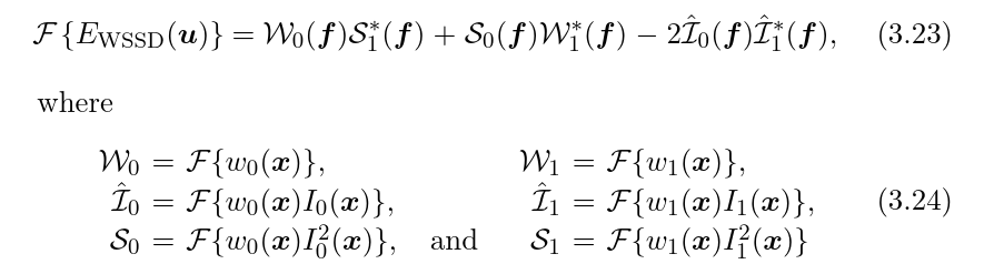
The 30x30 images gets padded with zeros to a 60x60s, then a masked by a 30x30 square of 1 weights (I initially planned to tune the weights some more, but didn’t). In the formula I0, I1 are the images and w0, w1 the weights.
With that done, what was left was just searching the minimum. The calculated offset of the minimum can then be passed to uinput to move the mouse!
Offset calculation can even be refined to sub-pixel accuracy by using interpolation (bicubic in my case). The gradient descent approach is supposedly better and faster, but I’m bad with numerics and couldn’t get it to work, so I just recursively checked offsets near the current estimate.
Because it’s sub-pixel, it is possible to multiply the offset and still be able to move 1 pixel, so the offset got multiplied by 16. That’s quite a lot and the cursor is shivering in fear of that extreme speed.
For comparison, the side-length of the video from the mouse you can see is roughly 0.5mm in the real world, and mouse acceleration is disabled.
Using the mouse this way is actually rather impractical, so I went back to using it normally.