A tour of my laptop's firmware
The Embedded Controller and Its Legacy
In this blog post I would like to write up a bit about the things going on in the embedded controller of my laptop. It is an 8051-based IT8586E built into an Lenovo Ideapad 310-15IKB laptop. But before going into the specifics, it might be useful to know what an embedded controller even is.
A Brief History of the Embedded Controller on x86 Platforms
In the beginning the IBM PC was created. This made a lot of people angry and was widely regarded as a bad move.
The board came with a bunch of peripherals like an Intel 8259 (programmable interrupt controller) or an Intel 8253 (programmable timer).
They could be addressed through the in/out instructions of the x86 core (and in fact the 8259 and 8253 still can be addressed on modern x86 CPUs, they are part of the CPU die itself now).
One of them, the Intel 8255 (programmable peripheral interface), was responsible for interfacing to the keyboard.
With the release of the IBM PC AT in 1984, the i8255 got replaced with an Intel 8042, which was a microcontroller responsible for communicating with the keyboard and is called the keyboard controller.
It got two addresses in the x86 I/O space, 0x60 and 0x64.
The x86 core could send commands to it and receive data over those ports.
The keyboard controller had some leftover pins, so IBM decided it was a bright idea to use those for purposes unrelated to the keyboard like resetting the PC.
Around the late 1980s, peripherals got more and more consolidated into single chips, like the northbridge and southbridge. One of the chips, the super I/O chip, was responsible for communicating with slower interfaces like serial/parallel ports and floppy disks. It also often included the keyboard controller.
For laptops, there was also a need for advanced power management. The laptop vendors looked at the keyboard controller and its ability to reset the PC and said: “This is great actually, let’s copy that design.” So two ports were added, with a similar command/data interface to the keyboard controller. Indeed, on many platforms, it ran on the same controller, residing in the Super I/O chip.
In the mid 1990s, ACPI (Advanced Configuration and Power Interface) became a thing. It defined a standardized interface for the EC: through its command interface, one would be able to access an 8-bit address space of vendor-defined variables. The variables could be defined in ACPI’s language AML and the AML could also contain code to update those variables.
In the late 2000s and 2010s, the northbridge and southbridge got merged into the CPU. (Note: The integration of the southbridge, or PCH/Platform Controller Hub, into the CPU appears to have only happened on mobile platforms). However, the EC is still in a separate chip on laptops, also containing the Super I/O functionality and the keyboard controller. It has tasks like
- controlling fans
- communicating with the Smart Battery subsystem
- reading out the keyboard matrix and the state of power buttons
- communicating with voltage regulators.
The Board Layout of my Laptop
Since the EC communicates a lot with hardware, it would be nice to know that hardware. Luckily, some random person put a boardview of the laptop onto a shady forum. A boardview shows the traces and components of a laptop’s mainboard, and can be quite daunting to look at since there are so many traces. I have tried to give a rough overview with this diagram of how things are connected (most power-related components are left out).
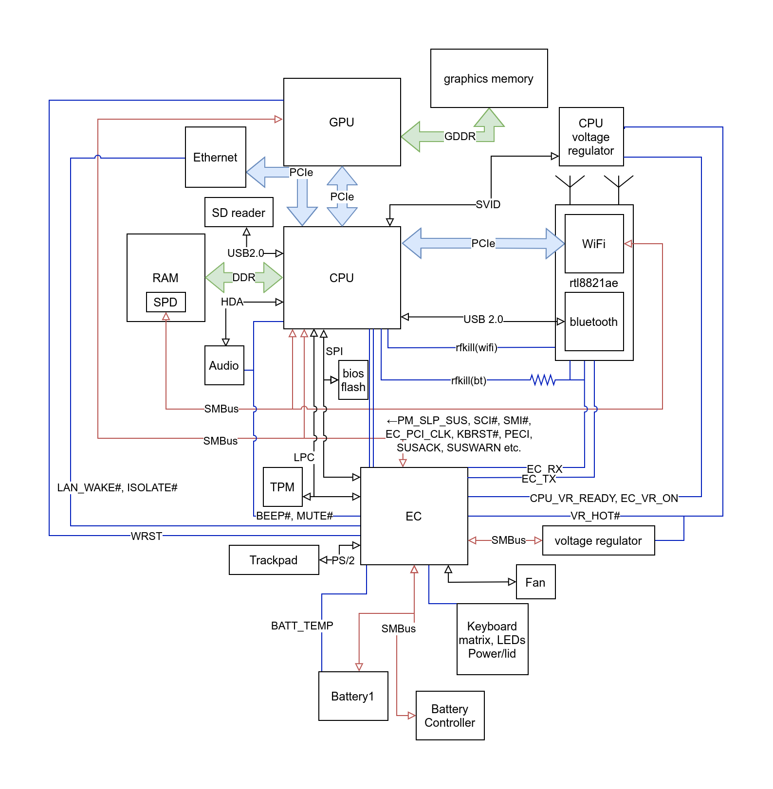
The CPU is connected to the EC over the LPC protocol, which is basically a low pin replacement for the ISA bus that was present on older PCs and most communication between the CPU and the EC happens over it. However, there are many traces (shown in blue and without arrows) between the EC and CPU which have specific purposes, like the SCI line for raising an interrupt from the EC in the CPU.
Also, there is a trace named BEEP# for making the laptop beep.
EC Firmware
The firmware is easily found: I had extracted the BIOS image previously for other purposes, and running cpu_rec on it returns roughly 160K of 8051 code right at the beginning of the image, before all the UEFI stuff starts. Now, 8051s have a 16-bit address space, so 160K of code does not fit into it, which means that the firmware is banked (meaning that parts of the firmware in the address space are swapped dynamically with other parts of the firmware by writing to some registers).
The size of the banked blocks is usually either 32K or 64K on most 8051s and one can usually figure out the size by looking at where stuff repeats, since there is usually some common code between the blocks (one quick way to see that would be to do an autocorrelation). On this firmware, it turns out to be 32K byte blocks.
Running at51 base on 32k blocks, one sees that the first block is loaded at 0x0, the second one at 0x8000, the third one at 0x8000 and the fourth one also at 0x8000, so the first 32K bytes of the address space stay the same and the higher 0x8000 are dynamically swapped between three possible banks.
The fifth bank does not contain any code but only some data.
At that point, I got the bright idea of actually looking up the datasheet for the part. I did not find the specific datasheet for the part, but the one for the IT8502E was close enough. Luckily, it details most of the I/O and seems to mostly match what the firmware does.
Browsing the datasheet, there is a mention of a I2EC functionality for debugging, however it is not documented.
Upon some searching, I found ECSpy, which is a rust implementation of it by system76, who are making their own EC firmware.
All it does is allow r/w access to the RAM and I/O registers of the EC. The I/O access has the further restriction that writing is only well-defined for flip-flop based registers (so for example, causing state-machine transitions would not work).
The datasheet also mentions that the debug functionality has to be enabled in a register, but it is indeed enabled. Access to it happens over the x86 I/O ports of the Super I/O functionality, so it is possible to use from user space without the need to write a driver.
Some specifications are also useful when trying to reverse engineer firmware that interact with those specifities. For this project, I read parts of the ACPI specification, SMBus and Smart Battery specifications. Along with the boardview, the datasheet, the various ghidra windows, a browser for looking at stuff like scancodes, the Linux kernel driver source for my EC, the disassembled ACPI machine code, the debug tool and its source, these many windows make it worth it to have more monitors for quickly cross-referencing stuff.
The firmware contains a single main function where most of the processing is done.
Typically, interrupts set some bits corresponding to events and those events get later processed outside of interrupt context in the main loop.
The controller has a number of different interrupts in the interrupt vector, but most interrupts go to the so-called INTC interrupt at address 0x13, where it jumps to a big jump tables that contains all the addresses for specific interrupt handlers.
A large amount of work is done by the part of the main loop triggered by a timer. The timer in the EC is programmed to generate an interrupt every 1ms. The ticks are then divided into events that happen every 10ms, every 50ms, every 1000ms etc. Updating ACPI variables is done mostly within this context.
POST Cards in Modern Laptops
When a x86 CPU boots, the BIOS regularly writes values to I/O port 0x80 to indicate its progress and also when errors occur.
These values were put onto the ISA bus in the past, where one could plug in a POST card which displayed the current value in hexadecimal so that one could diagnose boot issues.
With modern laptop, the LPC bus is the replacement for the ISA bus, and it still typically gets sent there.
The EC firmware actually has code to handle 0x80 port writes.
In that code path, one finds some code that decomposes the value into its nibbles and uses the nibbles as offset into the following table:
0xc0, 0xf9, 0xa4, 0xb0, 0x99, 0x92, 0x82, 0xf8, 0x80, 0x90, 0x88, 0x83, 0xc6, 0xa1, 0x86, 0x8e
It then serially outputs the resulting value, along with clock pulses, onto GPIO pins.
The lookup table might seem familiar: that is because it converts the nibbles into a hexadecimal digit for a 7-segment display.
If you look back at the board layout, there are two traces, EC_TX and EC_RX (the names are kind of misleading, since one of them is data and other is clock, both only used for sending).
They go to the wifi chip, which is connected through an m.2 connector.
However, they are not actually connected to anything on the wifi card.
This suggests that there is some POST card that can be plugged into an m.2 connector to debug boot issues. Since I know the protocol, i tried making my own version (basically two daisy-chained shift registers connected to the 7-segment displays). Look at how cute it is.

Unfortunately, I must have messed something up because it ended up not working and I did not really want to spend time to fix it.
The Keyboard Machinery
The PC gets the keystrokes of the laptop keyboard from the i8042 ports of the EC (0x60 and 0x64).
The EC has direct access to the keyboard matrix, thus it has to convert raw positions on the keyboard to PS/2 scancodes.
It also has to keep track of the Fn key, which defines alternate functions for some keys and does not get sent to the CPU.
One might think that this would be as easy as looking up a single lookup table and sending that to the host. Alas, PS/2 scancodes are a mess.
There are three different scancode sets which have no similarity, and the EC uses set 2. A single key press does not always generate a single byte of scancode.
Some examples:
- Pressing
xgenerates the scancode22. Releasing it generatesF0 22. - Pressing
Deletegenerates the scancodeE0 71. Releasing it generatesE0 F0 71.
Generally, most keys fall into this pattern, where releasing it is the same as pressing with a F0 prefix.
E0 is then a prefix for an extended scancode set (note that F0 comes after E0 for releasing a key).
There are some exceptions, for example:
- Pressing
Pause(which isFn + bon the laptop) generates the sequenceE1 14 77 E1 F0 14 F0 77. Releasing it does not generate anything. - However, pressing
Ctrl + Pausegenerates a completely unrelated sequence, namelyE0 7E E0 F0 7E. Releasing does nothing again. - There are some media keys like
Mute Microphone. These do not have a PS/2 scancode. Instead, the EC generates an SCI interrupt. The corresponding AML code in the ACPI tables then send a notify event to the OS. The OS then reads the state of the ACPI EC variables and generates the native events.
The positions of the key on the keyboard is a 7-bit integer, which is used as an index into a lookup table that converts it to an intermediate byte value. This first lookup table can be changed by i8042 commands to switch to a different layout.
If the value of the intermediate value is below 0x80, it just corresponds to a normal single-byte PS/2 scancode.
However for other values, they are used again as an index into a lookup table.
The resulting value defines the function that is used to handle the scancode.
The resulting scancodes are then put into a 16 byte circular buffer whose bytes are then sent to the host if possible.
There is also some other stuff going on, like anti-ghosting, debouncing, and the Fn key handling that I skipped over.
Interestingly, it also sometimes adds some scancodes to the buffer in places unrelated to keyboard stuff, like a Win+Q or a suspend key press.
I did not really analyze that further.
A Cryptic Piece of Code
When looking from afar at the firmware file, one notices that in the 4th block (0x18000-0x20000), there is not a lot of code.
Strangely, the code part is somewhere in the middle of otherwise 0xffs, with an extend of 0x1e000-0x1e596.
The first thought is that it is some kind of bootloading/flashing related stuff, but looking into the actual code this turns out to be false.
At a closer look, one is met with constants like 0x67452301, 0xEFCDAB89 or 0xCA62C1D6.
Those are constants used in SHA-1.
Why would an embedded controller need SHA-1? Looking at what calls the SHA-1 code, one finds it used in the communication with the battery over SMBus:
- The EC generates a random 20 bytes nonce and sends them to register
0x27of the battery - The EC calculates
sha1($secret . sha1($secret . nonce))where$secretis a 16-byte secret stored in the firmware - The EC reads 20 bytes from register
0x28of the battery and ensures it is the same as calculated in the previous step
So it appears that batteries are authenticated before being able to use them to prevent knockoffs or something.
Where is the Code Actually Stored
According to the datasheet, the firmware is able to access the flash contents in a linear way with a 28-bit address register and an 8-bit data register.
In the firmware one sees a lot of write and read accesses to addresses 0x0fff_fe00 and 0x0fff_fd00.
But the flash is far from 256M in size, so it is clearly does not access that address on flash.
A closer look at the code reveals that the code mostly writes 0xff to 0x0fff_fe00 and then writes/reads a bunch of bytes, like 0x05, 0x02 or 0xd7.
It turns out that these are SPI flash commands and this is the way that the firmware writes to and erases the flash.
However, looking at the image stored on the BIOS, there does not seem to be any difference to the original.
Are these difference maybe stored only in the cache (which the EC does have)?
Are the responsible code paths just not executed?
A lot 8051 firmware tends to have debug functionality programmed into it, and this one is not different. Behind the Keyboard Controller commands and EC commands, there are a lot of functions that are clearly for debugging. One of them is a keyboard controller command to read flash addresses using the register from inside the EC.
Dumping the firmware from that, one does get an image that differs from the original. I initially assumed that the EC used the image on the BIOS flash, since it is stored there and the EC is connected to the flash. However in retrospect that does not really make sense: both the CPU and the EC are connected to it without anything in between, so one would inevitably get bus conflicts if both try to read from it. The firmware is actually stored in the EC itself, a feature not present in the IT8502 (which furthered my confusion since I used that datasheet for reference).
Executing my own Code on the EC
It might be worth mentioning that 8051 has a bunch of different address spaces:
- IRAM: 256 bytes of internal ram (fast)
- SFR: 128 bytes of I/O on the upper half of IRAM (falls back to IRAM on indirect memory addresses)
- XDATA: 16-bit addressable external RAM (slow and also contains I/O on this EC)
- CODE: 16-bit addressable code space
Notably, there is no instruction to write to CODE space. However, as seen in the previous section, writing to flash is a possible way to change the CODE space.
But I did not want to do that, since that comes with a risk of bricking the device. The EC has a way of reprogramming it by using the inputs/outputs from the keyboard matrix as a parallel port, but I did not want to do that.
Another issue with writing to flash is that it is checksummed. The firmware has a signature which indicates where it starts, and in it are two bytes that change seemingly randomly across revision of the firmware. This usually happens with checksums. If that is the case, it is not clear where the checksum would start and end and how it is calculated.
Using delsum part (a tool I made earlier for exactly this kind of stuff), one finds multiple candidates:
it is a CRC with polynomial 0x8005 and the checksum ends on 0x1ffff.
However the start can not be reliably determined, since all revisions I could find are same before address 0x4000
This means that for each starting offset before 0x4000, there is a possible set of checksum parameters that result in all the right checksums.
It still allows to change bytes within the checksummed region as long as one is sure it is really part of the region, since only the end of the checksummed region is important for that.
There is not actually a need to write to flash to execute custom code though.
The EC also has another way:
Addresses from 0x0000-0x1000 in XDATA are regular RAM and can be mapped to arbitrary locations in CODE space by writing to some registers.
So executing custom code should be as easy as mapping one of these over existing code.
The ram from 0x0000-0x0e00 is used by the firmware, so the ones that are left are block 3 and 4, both 256 bytes.
However in order to map those, one still has to write to the registers and the ram in the XDATA. There is a debug function that writes to custom in XDATA, but it is buggy and can only write to addresses where the top byte is the same as the bottom byte of the address. There is also I2EC, which is good enough for writing to the SRAM.
I was hesitant about letting it write to I/O, since it was mentioned that it only works properly for flip flops. But in the mapping registers there is also a bit to start a DMA transaction (because of course this chip also has DMA). In any case, there is no way to verify that it maps the way I want it to, since there is no debug function to read from CODE space.
Luckily there is another way: it also uses the mapping functionality for rewriting the flash (since you do not want it to crash when it reaches the code that is doing the writing). Using the I2EC functionality, one can change the SRAM in the XDATA to contain some debug functionality and change the flashing routine to point to the debug functionality.
That way, I could now also verify that mapping works as intended.
And that way, I found out that mapping does not work as intended.
It appears that e.g. mapping XDATA 0x0e00-0x0f00 to 0x7722 maps address 0x7722 to 0x0e22 (and not 0x0e00), 0x7723 to 0x023, address 0x7800 to 0x0e00 and address 0x7821 to 0x0e21.
This is presumably a bug in the silicon.
In any case it is easy to work around, since this is still a bijection and one can just write the code to the corresponding places into the XDATA. And it turns out that I2EC writes directly to the mapping registers works too, so I did not need to invoke the flashing mode to execute debug code and then write it.
I proceeded to make a program that takes an ihex file and sets up the pages 0xe00 and 0xf00 so that i could just specify the patch locations with ORG instructions in the assembly and the program would do the rest of filling the unpatched locations with the firmware from the image and writing the code correctly into the SRAM.
This reduces developer friction and makes the development process more agile or something.
End
This is it for this blog post, in the next blog post I will be poking around in the firmware of the wifi module (rtl8821ae) and also build a small keylogger.